DSSSB TGT / PGT · Computer Science

Digital Logic & Number Systems Previous Year Questions (page 4)

190 Digital Logic & Number Systems (Computer Science) questions asked in DSSSB TGT / PGT previous year papers, each with the correct answer and explanation. Read them free on UTpaper, or attempt the full papers as timed online tests.

  • 190 questions
  • Official answer key
  • Free

Other Computer Science topics

Q151DSSSB TGT Computer Science (Technical), 12 Sep 2025, Shift 3 (5:00 PM)
In which logic gate, if any input is low, then the output will be high?
  1. AXNOR Logic Gate
  2. BAND Logic gate
  3. CNOR Logic gate
  4. DNAND Logic Gate
Show answerHide answer

Correct answer: (D) NAND Logic Gate

Explanation

A NAND gate outputs 0 only when all inputs are 1, so if any input is 0 (low) the output is 1 (high). An AND gate would give 0 in that case.

Q152DSSSB TGT Computer Science (Technical), 12 Sep 2025, Shift 3 (5:00 PM)
If a, b are the inputs and y is the output of a two input AND logic gate, then which of the following is the correct expression for the output of the AND logic gate?
  1. Ay = a'.b'
  2. By = a.b'
  3. Cy = a'.b
  4. Dy = a.b
Show answerHide answer

Correct answer: (D) y = a.b

Explanation

An AND gate gives 1 only when both inputs are 1, so y = a·b. The options with complemented inputs describe other functions.

Q153DSSSB TGT Computer Science (Technical), 12 Sep 2025, Shift 3 (5:00 PM)
Convert the hexadecimal number (A5) 16 to its decimal equivalent.
  1. A165
  2. B160
  3. C175
  4. D170
Show answerHide answer

Correct answer: (A) 165

Explanation

(A5)₁₆ = 10 × 16 + 5 = 160 + 5 = 165.

Q154DSSSB TGT Computer Science (Technical), 12 Sep 2025, Shift 3 (5:00 PM)
Which of the following is NOT a part of the internal architecture of the Central Processing Unit (CPU)?
  1. ARegister
  2. BRandom Access Memory
  3. CControl Unit
  4. DArithmetic Logic Unit
Show answerHide answer

Correct answer: (B) Random Access Memory

Explanation

The CPU contains registers, the control unit and the ALU. RAM is main memory, which sits outside the CPU and is reached over the bus.

Q155DSSSB TGT Computer Science (Technical), 12 Sep 2025, Shift 2 (1:00 PM)
Convert the decimal number 325 to its octal equivalent.
  1. A514
  2. B485
  3. C541
  4. D505
Show answerHide answer

Correct answer: (D) 505

Explanation

325 / 8 = 40 remainder 5, 40 / 8 = 5 remainder 0, 5 / 8 = 0 remainder 5. Reading remainders bottom up gives 505 in octal (5 x 64 + 0 + 5 = 325).

Q156DSSSB TGT Computer Science (Technical), 12 Sep 2025, Shift 2 (1:00 PM)
Convert the binary number (11011) 2 to its decimal equivalent.
  1. A29
  2. B27
  3. C31
  4. D25
Show answerHide answer

Correct answer: (B) 27

Explanation

11011 = 16 + 8 + 0 + 2 + 1 = 27.

Q157DSSSB TGT Computer Science (Technical), 12 Sep 2025, Shift 2 (1:00 PM)
Which addressing mode uses the actual address of the data in the instruction?
  1. AIndirect addressing
  2. BImmediate addressing
  3. CDirect addressing
  4. DRegister addressing
Show answerHide answer

Correct answer: (C) Direct addressing

Explanation

In direct (absolute) addressing, the instruction's address field holds the actual memory address of the operand. Immediate addressing holds the data itself and indirect holds the address of the address.

Q158DSSSB TGT Computer Science (Technical), 12 Sep 2025, Shift 1 (9:00 AM)
Which of the following statements is false about universal logic gates?
  1. AAll basic logic gates can be implemented through universal logic gates.
  2. BNOR gate is known as universal logic gate.
  3. CNAND gate is known as universal logic gate.
  4. DAll basic logic gates cannot be implemented using universal logic gates.
Show answerHide answer

Correct answer: (D) All basic logic gates cannot be implemented using universal logic gates.

Explanation

NAND and NOR are universal gates precisely because AND, OR and NOT (and hence every other gate) can be built from them alone, so the statement that basic gates cannot be built from them is false.

Q159DSSSB TGT Computer Science (Technical), 12 Sep 2025, Shift 1 (9:00 AM)
What is the 2’s complement of the binary number 1100?
  1. A0100
  2. B1111
  3. C11
  4. D1001
Show answerHide answer

Correct answer: (A) 0100

Explanation

Invert 1100 to get 0011, then add 1: 0011 + 1 = 0100.

Q160DSSSB TGT Computer Science (Technical), 12 Sep 2025, Shift 1 (9:00 AM)
Which of the following statements is false about simplification of Boolean functions using Karnaugh Map technique?
  1. AKarnaugh Map technique is used to simplify Product of Sum (POS) form of Boolean functions.
  2. BIn Karnaugh Map, the rows and columns are represented in binary code sequence.
  3. CIn Karnaugh Map, you group adjacent squares in the form of power of two and try to cover as many minterms or maxterms as you can in one group.
  4. DKarnaugh Map technique is used to simplify Sum of Product (SOP) form of Boolean functions.
Show answerHide answer

Correct answer: (B) In Karnaugh Map, the rows and columns are represented in binary code sequence.

Explanation

In a K-map, rows and columns are labelled in Gray code (00, 01, 11, 10) so adjacent cells differ by one bit; plain binary order (00, 01, 10, 11) would break adjacency. K-maps simplify both SOP and POS forms.

Q161DSSSB TGT Computer Science (Technical), 12 Sep 2025, Shift 1 (9:00 AM)
Which logical operation does the ALU perform that results in a 1 output only when both inputs are different?
  1. AAND
  2. BXOR
  3. COR
  4. DNOR
Show answerHide answer

Correct answer: (B) XOR

Explanation

XOR gives 1 only when its inputs differ (0,1 or 1,0) and 0 when they are the same. AND needs both 1, OR needs at least one 1.

Q162DSSSB TGT Computer Science, 25 Jun 2023, Shift 1 (8:30 AM)
Which of the following is NV RAM memory that retains its data even when turned off?
  1. ACache memory
  2. BFlash memory
  3. CRegister memory
  4. DMain memory
Show answerHide answer

Correct answer: (B) Flash memory

Explanation

Flash memory is non-volatile (NVRAM-type) memory that keeps its data without power, as in pen drives and SSDs. Cache, registers and main RAM are volatile.

Q163DSSSB TGT Computer Science, 25 Jun 2023, Shift 1 (8:30 AM)
Which of the following algebraic functions represents NAND gate?
  1. A(xy)'
  2. B(x+y)'
  3. Cx+y
  4. Dx*y
Show answerHide answer

Correct answer: (A) (xy)'

Explanation

NAND is NOT-AND, so its output is (xy)'. (x+y)' is NOR, x+y is OR and xy is AND.

Q164DSSSB TGT Computer Science, 25 Jun 2023, Shift 1 (8:30 AM)
The semiconductor memory Dynamic RAM (DRAM) stores each bit of information in a/an ______.
  1. Adiode
  2. Belectrical capacitor
  3. Cflip-flop
  4. Dresistor
Show answerHide answer

Correct answer: (B) electrical capacitor

Explanation

A DRAM cell stores each bit as charge on a tiny capacitor (with one transistor), which must be refreshed regularly. SRAM uses flip-flops.

Q165DSSSB TGT Computer Science, 25 Jun 2023, Shift 1 (8:30 AM)
What is the binary equivalent of the decimal number 10.25?
  1. A1010.01
  2. B1011.01
  3. C1101.01
  4. D1111.01
Show answerHide answer

Correct answer: (A) 1010.01

Explanation

10 = 1010₂, and 0.25 × 2 = 0.5 → 0, 0.5 × 2 = 1.0 → 1, so 0.25 = .01₂. Hence 10.25 = 1010.01₂.

Q166DSSSB TGT Computer Science, 24 Jun 2023, Shift 3 (4:30 PM)
The decimal equivalent of the binary number 111111 is:
  1. A46
  2. B63
  3. C52
  4. D36
Show answerHide answer

Correct answer: (B) 63

Explanation

111111₂ = 32 + 16 + 8 + 4 + 2 + 1 = 63 (that is, 2⁶ − 1).

Q167DSSSB TGT Computer Science, 24 Jun 2023, Shift 3 (4:30 PM)
Which of the following statements is true about Home Location Register (HLR) and Visitor Location Register (VLR)?
  1. AVLR is not responsible for the MS (Mobile Station) to inform the MLR about location changes.
  2. BVLR is not responsible for the MS (Mobile Station) to inform the HLR about location changes.
  3. CVLR is responsible for the MS (Mobile Station) to inform the HLR about location changes.
  4. DHLR is responsible for the MS (Mobile Station) to inform the VLR about location changes.
Show answerHide answer

Correct answer: (C) VLR is responsible for the MS (Mobile Station) to inform the HLR about location changes.

Explanation

When a mobile station enters a new area, the serving VLR registers it and informs the HLR of the location change, so the HLR always knows which VLR area the subscriber is in.

Q168DSSSB TGT Computer Science, 24 Jun 2023, Shift 3 (4:30 PM)
A Mod-6 counter and a Mod-S counter in cascade give a counter.
  1. AMod-14
  2. BMod-68
  3. CMod-2
  4. DMod-48
Show answerHide answer

Correct answer: (D) Mod-48

Explanation

Cascading counters multiplies their moduli: 6 × 8 = 48, giving a Mod-48 counter.

Q169DSSSB TGT Computer Science, 24 Jun 2023, Shift 3 (4:30 PM)
If two dice are thrown, find the probability that the sum is neither 5 nor 9?
  1. A3/9
  2. B5/9
  3. C1/9
  4. D7/9
Show answerHide answer

Correct answer: (D) 7/9

Explanation

A sum of 5 occurs 4 ways and a sum of 9 occurs 4 ways out of 36, so P(5 or 9) = 8/36 = 2/9. The required probability is 1 − 2/9 = 7/9.

Q170DSSSB TGT Computer Science, 24 Jun 2023, Shift 3 (4:30 PM)
Which of the following is an addressing mode used in an instruction of the form ADD R1, [R2]?
  1. ARegister Indirect
  2. BRegister
  3. CIndexed Register
  4. DAssembly Register
Show answerHide answer

Correct answer: (A) Register Indirect

Explanation

In ADD R1, [R2] the operand's address is held in register R2, which is register indirect addressing.

Q171DSSSB TGT Computer Science, 24 Jun 2023, Shift 3 (4:30 PM)
For what minimum value of propagation delay in each FF will a 10-bit ripple counter skip a count when it is clocked at 10 MHz?
  1. A10 ns
  2. B25 ns
  3. C100 ns
  4. D50 ns
Show answerHide answer

Correct answer: (A) 10 ns

Explanation

The ripple counter fails when the total delay of 10 flip-flops reaches the clock period: 10 × t_pd = 1/10 MHz = 100 ns, so t_pd = 10 ns.

Q172DSSSB TGT Computer Science, 7 Feb 2024, Shift 2 (12:30 PM)
Using K-map, simplify the Boolean function: F(x, y, z) = S (0, 2, 4, 5, 6) Which of the following is simplified function?
  1. AF = z + x'y'
  2. BF = z' + xy'
  3. CF = z + x'y
  4. DF = z' + xy
Show answerHide answer

Correct answer: (B) F = z' + xy'

Explanation

Minterms 0, 2, 4, 6 (all with z = 0) group into z'. Minterms 4 and 5 (x = 1, y = 0) group into xy'. So F = z' + xy'.

Q173DSSSB TGT Computer Science, 7 Feb 2024, Shift 2 (12:30 PM)
Which of the following part of the CPU has the necessary electronic circuitry to perform binary addition and shift operations in computer system?
  1. AArithmetic Logic Unit (ALU)
  2. BMemory Buses
  3. CRegisters
  4. DControl Unit
Show answerHide answer

Correct answer: (A) Arithmetic Logic Unit (ALU)

Explanation

The ALU contains the circuits for arithmetic (such as binary addition), logic and shift operations. The control unit only directs operations.

Q174DSSSB TGT Computer Science, 7 Feb 2024, Shift 2 (12:30 PM)
In which of the following type of addressing mode, the instruction specifies a register in the CPU whose contents give the address of the operand in memory?
  1. ARegister indirect mode
  2. BIndirect address mode
  3. CImplied mode
  4. DImmediate mode
Show answerHide answer

Correct answer: (A) Register indirect mode

Explanation

In register indirect mode the chosen register holds the memory address of the operand, not the operand itself.

Q175DSSSB TGT Computer Science, 7 Feb 2024, Shift 2 (12:30 PM)
Which of the following statement(s) is/are correct regarding Assembly language? I. An assembler converts (or assembles) the symbolic program of an Assembly language into its equivalent machine program. II. A program written in an assembly language is machine dependent.
  1. ABoth I and II
  2. BOnly II
  3. COnly I
  4. DNeither I nor II
Show answerHide answer

Correct answer: (A) Both I and II

Explanation

An assembler translates assembly mnemonics into machine code, and because assembly instructions map to a specific processor's instruction set, the program is machine dependent. Both are true.

Q176DSSSB TGT Computer Science, 7 Feb 2024, Shift 2 (12:30 PM)
Which of the following Instruction format use an implied accumulator (AC) register for all data manipulation?
  1. AOne-address instructions
  2. BT hree-address instructions
  3. CZero-address instructions
  4. DTwo-address instructions
Show answerHide answer

Correct answer: (A) One-address instructions

Explanation

One-address instructions use an implied accumulator (AC) for all data manipulation, e.g. ADD X means AC = AC + M[X].

Q177DSSSB TGT Computer Science, 7 Feb 2024, Shift 2 (12:30 PM)
In CPU, which of the following type of register is required by the control unit and contains the instruction currently being executed?
  1. AInstruction register
  2. BAccumulator
  3. CProgram register
  4. DMemory data register
Show answerHide answer

Correct answer: (A) Instruction register

Explanation

The Instruction Register (IR) holds the instruction currently being decoded and executed, for use by the control unit.

Q178DSSSB TGT Computer Science, 7 Feb 2024, Shift 2 (12:30 PM)
Which of the following statement is correct regarding point-to-point connection in the data communication? I. It provides a dedicated link between two devices. II. It is a timeshared connection.
  1. AOnly II
  2. BBoth I and II
  3. CNeither I nor II
  4. DOnly I
Show answerHide answer

Correct answer: (D) Only I

Explanation

A point-to-point connection gives a dedicated link between exactly two devices. A shared, timeshared link describes a multipoint connection, so only I is correct.

Q179DSSSB TGT Computer Science, 7 Feb 2024, Shift 2 (12:30 PM)
The E-waste (management) rules 2016 of India, recognizes two broad categories: IT and telecommunication equipment and consumer electrical and electronics including which of the following material? I. Fluorescent II. Mercury
  1. AOnly I
  2. BOnly II
  3. CBoth I and II
  4. DNeither I nor II
Show answerHide answer

Correct answer: (C) Both I and II

Explanation

The E-Waste (Management) Rules 2016 cover IT and telecom equipment and consumer electrical and electronics, and also include compact fluorescent lamps (CFL) and other mercury-containing lamps. So both apply.

Q180DSSSB TGT Computer Science, 7 Feb 2024, Shift 2 (12:30 PM)
Which of the following is commonly used in UNICODE encoding schemes and number system in computer science?
  1. AUT F-17
  2. BUT F-61
  3. CUT F-8
  4. DUT F-35
Show answerHide answer

Correct answer: (C) UT F-8

Explanation

UTF-8 is the most widely used Unicode encoding; it uses 1 to 4 bytes per character and is ASCII-compatible. UTF-17, 61 and 35 do not exist.

Q181DSSSB TGT Computer Science, 7 Feb 2024, Shift 2 (12:30 PM)
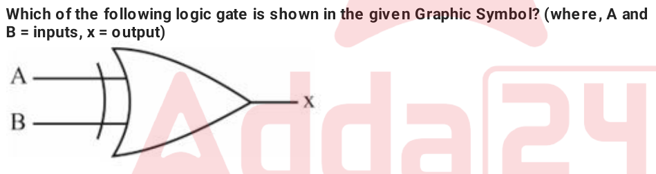
Which of the following logic gate is shown in the given Graphic Symbol? (where, A and B = inputs, x = output)
  1. AOR gate
  2. BNAND gate
  3. CNOR gate
  4. DExclusive – OR (XOR) gate
Show answerHide answer

Correct answer: (D) Exclusive – OR (XOR) gate

Explanation

The gate shown has an extra curved line at the input side of the OR shape, which is the symbol for the Exclusive-OR (XOR) gate.

Q182DSSSB TGT Computer Science, 7 Feb 2024, Shift 2 (12:30 PM)
Number with decimal points is called ______ in programming language.
  1. AFractional point numbers
  2. BComplex numbers
  3. CImaginary Numbers
  4. DInteger
Show answerHide answer

Correct answer: (A) Fractional point numbers

Explanation

Numbers with a decimal point (like 3.14) are fractional/floating point numbers, stored as float in Python. Integers have no decimal part.

Q183DSSSB TGT Computer Science, 7 Feb 2024, Shift 2 (12:30 PM)
ASCII (American Standard Code for Information Interchange) can only handle ______ or at most ______ languages and that shows its limitation to handle all world languages.
  1. A2, 5
  2. B1, 2
  3. C1, 5
  4. D3, 4
Show answerHide answer

Correct answer: (B) 1, 2

Explanation

ASCII uses 7 bits (128 characters), enough mainly for English, so it can handle only one, or at most two, languages.

Q184DSSSB TGT Computer Science, 7 Feb 2024, Shift 2 (12:30 PM)
Which of the following statement(s) is/are correct regarding AND logic gate? I. The AND gate produces the output value 1 if input A and input B are both equal to 1. II. The algebraic operation symbol of the AND function is the same as the multiplication symbol of ordinary arithmetic.
  1. ANeither I nor II
  2. BOnly I
  3. CBoth I and II
  4. DOnly II
Show answerHide answer

Correct answer: (C) Both I and II

Explanation

AND outputs 1 only when both inputs are 1, and it is written with the multiplication symbol (A·B). Both are correct.

Q185DSSSB TGT Computer Science, 7 Feb 2024, Shift 2 (12:30 PM)
Unicode in the programming language can be represented using which of the bit format standards in computer science?
  1. A8-bit
  2. B17-bit
  3. C65-bit
  4. D9-bit
Show answerHide answer

Correct answer: (A) 8-bit

Explanation

Unicode can be encoded with 8-bit code units, as in UTF-8 (UTF-16 and UTF-32 also exist). 17, 65 and 9-bit formats are not standards.

Q186DSSSB TGT Computer Science, 25 Jun 2023, Shift 3 (4:30 PM)
Which of the following is an example of a combinational circuit?
  1. ACounter
  2. BShift Register
  3. CClock
  4. DEncoder
Show answerHide answer

Correct answer: (D) Encoder

Explanation

An encoder's output depends only on its present inputs, so it is a combinational circuit. Counters and shift registers have memory, which makes them sequential.

Q187DSSSB TGT Computer Science, 25 Jun 2023, Shift 3 (4:30 PM)
What would be the 2's complement representation of the —15 decimal value?
  1. A1001
  2. B1111111
  3. C1111
  4. D10001
Show answerHide answer

Correct answer: (C) 1111

Explanation

Note: the answer key gives (C), but 1111 is −1 in 4-bit two's complement, and −15 cannot fit in 4 bits. With 5 bits, 15 = 01111, so −15 = 10001 (option D).

Q188DSSSB TGT Computer Science, 25 Jun 2023, Shift 2 (12:30 PM)
How many INVALID input combinations occur at the input of a BCD adder?
  1. A58
  2. B56
  3. C156
  4. D256
Show answerHide answer

Correct answer: (C) 156

Explanation

Two 4-bit inputs give 2⁸ = 256 combinations. Only 10 × 10 = 100 are valid BCD digit pairs (0-9 each), so 256 − 100 = 156 combinations are invalid.

Q189DSSSB TGT Computer Science, 25 Jun 2023, Shift 2 (12:30 PM)
A register contains a 3's complement number 10100. If it is divided by 2, find the value of the register.
  1. A01100
  2. B00110
  3. C01010
  4. D11010
Show answerHide answer

Correct answer: (C) 01010

Explanation

Dividing by 2 is done by shifting the register one bit to the right: 10100 becomes 01010 (20 ÷ 2 = 10).

Q190DSSSB TGT Computer Science, 25 Jun 2023, Shift 2 (12:30 PM)
What is the size of the computer accumulator register?
  1. A8 bytes
  2. B16 bytes
  3. C8 KB
  4. D4 bytes
Show answerHide answer

Correct answer: (D) 4 bytes

Explanation

The accumulator's size equals the processor's word length. For a 32-bit processor it is 32 bits = 4 bytes.

How to use these DSSSB TGT / PGT Computer Science questions

Every question here was asked in a real DSSSB TGT / PGT paper; the paper and shift are shown on the card, and the number opens the question on its own page. Try each one before tapping Show answer, then attempt the full DSSSB TGT / PGT papers as timed tests to check your speed under exam conditions.
More DSSSB TGT / PGT subjects